- 您现在的位置:买卖IC网 > Sheet目录474 > MAX3541EVKIT+ (Maxim Integrated)KIT FOR MAX3541 DVB TUNER
�� �
�
�Complete� Single-Conversion�
�Television� Tuner�
�Write� Cycle�
�When� addressed� with� a� write� command,� the� MAX3541�
�allows� the� master� to� write� to� a� single� register� or� to� multi-�
�ple� successive� registers.�
�A� write� cycle� begins� with� the� bus� master� issuing� a�
�START� condition� followed� by� the� seven� slave� address�
�bits� and� a� write� bit� (R/� W� =� 0).� The� MAX3541� issues� an�
�ACK� if� the� slave� address� byte� is� successfully� received.�
�The� bus� master� must� then� send� to� the� slave� the�
�address� of� the� first� register� it� wishes� to� write� to.� If� the�
�slave� acknowledges� the� address,� the� master� can� then�
�write� one� byte� to� the� register� at� the� specified� address.�
�Data� is� written� beginning� with� the� most� significant� bit.�
�The� MAX3541� again� issues� an� ACK� if� the� data� is� suc-�
�cessfully� written� to� the� register.� The� master� can� contin-�
�ue� to� write� data� to� the� successive� internal� registers� with�
�the� MAX3541� acknowledging� each� successful� transfer,�
�or� it� can� terminate� transmission� by� issuing� a� STOP� con-�
�dition.� The� write� cycle� does� not� terminate� until� the� mas-�
�ter� issues� a� STOP� condition.�
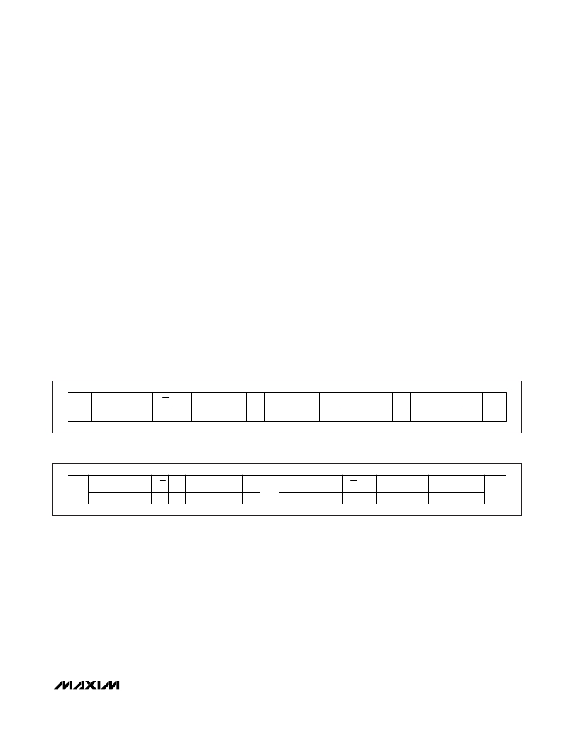
�Figure� 2� illustrates� an� example� in� which� registers� 0�
�through� 2� are� written� with� 0x0E,� 0xD8,� and� 0xE1,�
�respectively.�
�Read� Cycle�
�A� read� cycle� begins� with� the� bus� master� issuing� a�
�START� condition� followed� by� the� seven� slave� address�
�bits� and� a� write� bit� (R/� W� =� 0).� The� MAX3541� issues� an�
�ACK� if� the� slave� address� byte� is� successfully�
�received.� The� master� then� sends� the� 8-bit� address� of�
�the� first� register� that� it� wishes� to� read.� The� MAX3541�
�then� issues� another� ACK.� Next,� the� master� must� issue�
�a� START� condition� followed� by� the� 7� slave� address�
�bits� and� a� read� bit� (R/� W� =� 1).� The� MAX3541� issues� an�
�ACK� if� it� successfully� recognizes� its� address� and�
�begins� sending� data� from� the� specified� register�
�address� starting� with� the� most� significant� bit� (MSB).�
�Data� is� clocked� out� of� the� MAX3541� on� the� rising�
�edge� of� SCL.� On� the� 9th� rising� edge� of� SCL,� the� mas-�
�ter� can� issue� an� ACK� and� continue� reading� succes-�
�sive� registers� or� it� can� issue� a� NACK� followed� by� a�
�STOP� condition� to� terminate� transmission.� The� read�
�cycle� does� not� terminate� until� the� master� issues� a�
�STOP� condition.� Figure� 3� illustrates� an� example� in�
�which� registers� 0� and� 1� are� read� back.�
�START�
�WRITE� DEVICE�
�ADDRESS�
�11000[ADDR2][ADDR1]�
�R/W�
�0�
�ACK�
�—�
�WRITE� REGISTER�
�ADDRESS�
�0x00�
�ACK�
�—�
�WRITE� DATA� TO�
�REGISTER� 0x00�
�0x0E�
�ACK�
�—�
�WRITE� DATA� TO�
�REGISTER� 0x01�
�0xD8�
�ACK�
�—�
�WRITE� DATA� TO�
�REGISTER� 0x02�
�0xE1�
�ACK�
�—�
�STOP�
�Figure� 2.� Example:� Write� Registers� 0� Through� 2� with� 0x0E,� 0xD8,� and� 0xE1,� Respectively�
�START�
�WRITE� DEVICE�
�ADDRESS�
�110000[ADDR2][ADDR1]�
�R/W� ACK�
�0�
�—�
�WRITE� 1ST� REGISTER�
�ADDRESS�
�0x00�
�ACK�
�—�
�START�
�WRITE� DEVICE�
�ADDRESS�
�110000[ADDR2][ADDR1]�
�R/W� ACK�
�1� —�
�READ� DATA�
�REG� 0�
�D7–D0�
�ACK�
�—�
�READ� DATA�
�REG� 1�
�D7–D0�
�NACK�
�—�
�STOP�
�Figure� 3.� Example:� Read� Data� from� Registers� 0� and� 1�
�______________________________________________________________________________________�
�15�
�发布紧急采购,3分钟左右您将得到回复。
相关PDF资料
MAX3542CLM+
IC TV TUNER SGL CONV 48LFCGA
MAX3542EVKIT+
KIT FOR MAX3542 DVB TUNER
MAX3543EVKIT+
EVAL KIT MAX3543
MAX3558EVKIT
EVAL KIT MAX3558
MAX4000EUA+T
IC CNTRLR RF-DETECT 8-MSOP
MAX4001EVKIT
EVAL KIT FOR MAX4001
MAX4003EUA+T
IC LOG AMP RF DETECT 45DB 8-MSOP
MAX44007EDT+T
SENSOR AMBIENT LIGHT 6UTDFN
相关代理商/技术参数
MAX3542CLM+
功能描述:调谐器 Single-Conversion Television Tuner RoHS:否 制造商:NXP Semiconductors 功能: 噪声系数: 工作电源电压: 最小工作温度: 最大工作温度:
MAX3542CLM+T
功能描述:调谐器 DVB Tuner RoHS:否 制造商:NXP Semiconductors 功能: 噪声系数: 工作电源电压: 最小工作温度: 最大工作温度:
MAX3542EVKIT+
功能描述:射频开发工具 MAX3542 Eval Kit RoHS:否 制造商:Taiyo Yuden 产品:Wireless Modules 类型:Wireless Audio 工具用于评估:WYSAAVDX7 频率: 工作电源电压:3.4 V to 5.5 V
MAX3543CTL+
功能描述:调谐器 Broadband Analog & Digital TV Tuner RoHS:否 制造商:NXP Semiconductors 功能: 噪声系数: 工作电源电压: 最小工作温度: 最大工作温度:
MAX3543CTL+T
功能描述:调谐器 Broadband Analog & Digital TV Tuner RoHS:否 制造商:NXP Semiconductors 功能: 噪声系数: 工作电源电压: 最小工作温度: 最大工作温度:
MAX3543EVKIT+
功能描述:射频开发工具 MAX3542/3 Eval Kit RoHS:否 制造商:Taiyo Yuden 产品:Wireless Modules 类型:Wireless Audio 工具用于评估:WYSAAVDX7 频率: 工作电源电压:3.4 V to 5.5 V
MAX3544CTL+
制造商:Maxim Integrated Products 功能描述:EVKIT FOR DIGITAL TV TUNER - Rail/Tube
MAX3544CTL+T
制造商:Maxim Integrated Products 功能描述:MULTIBAND DIGITAL TELEVISION TUNER - Tape and Reel